
Firmware security 3: Digging into System management mode (SMM)
In the third part of the series we are going to discuss System management mode (SMM) and it's security. Moreover, We will try to interact with the SMM from our linux system.

Skipping the part 2 of firmware security series, I have decided to jump directly on part 3 where we will learn about SMM (System management mode) and its security.
Game of privilege rings
If you have previous experience with OS Internals or security than you must have heard about traditional ring level, this includes ring 0(kernel mode), ring 3(usermode) and all privilege ring(1 and 2) between them. Here, low ring level define more privilege. But in intel architecture(also true for AMD architecture) the privilege ring doesn't end at ring 0 but goes much lower than that. Below is the representation of known ring level in intel architecture.
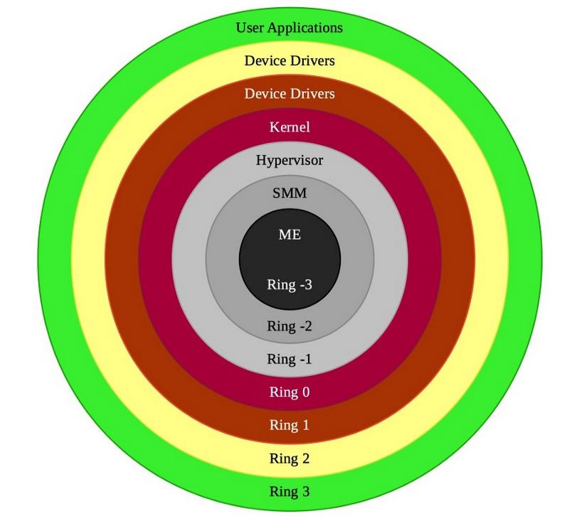
From the above ring levels, we are interested in digging into the ring -2 which is SMM. We care about SMM since its more privilege than not only the kernel mode but also hypervisor. A malicious code running with this privilege is OS independent and can survive OS reinstallation or disk wipes. Not only that, in general it's not possible to detect a malicious code running in SMM from the operating system.
What is System management mode (SMM)
System Management mode (SMM) is a relatively obscure mode on Intel processors, used for low-level hardware control. According to intel's documentation, SMM is a special-purpose operating mode provided for handling system-wide functions like power management, system hardware control, or proprietary OEM-designed code. It is intended for use only by system firmware, not by applications software or general-purpose system software. The main benefit of SMM is that it offers a distinct and easily isolated processor environment that operates transparently to the operating system or executive and applications. I.E when a processor enters SMM mode, all running tasks in all processors are suspended until the processor exits this mode.
Entering and Exiting System Management Mode
SMM can be invoked by signalling a System Management Interrupt (SMI). SMI can be generated by Hardware using SMI# pins in processor or by using local or I/O APIC busses. SMI can also be generated from software by writing to certain I/O ports or chipset registers. SMI cannot be masked like normal interrupts. Also, inside SMM all other interrupts are disabled.
To exit to SMM, cpu use RSM instruction. RSM can only be called from SMM. This instruction causes the processor to reload the saved context of the processor, switch back to protected or real mode, and resume executing the interrupted application or operating system program or task.
Generating SMI from linux
If you check your processors PCH/ICH datasheet, you will find that you can generate SMI using Advance Power Management (APM).
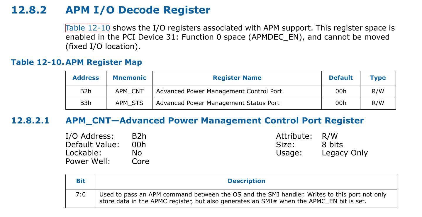
APM_CNT is control register present at I/O port 0xB2. Writing a byte to APM_CNT will generate a SMI. Let's try to do that from a linux driver.
static int my_init(void)
{


    uint8_t smm_response  = 0x0;
    printk(KERN_INFO "Hello world.\n");

    //check the initial value recieve from 0xB2 port
	smm_response = inb(0xb2);

	printk(KERN_INFO "data recieved from port 0xb2 is %x.\n", smm_response);
	//write to 0xB2 port to cause SMI
	outb(0x80, 0xb2);
	// Check the respose
	smm_response = inb(0xb2);

	printk(KERN_INFO "data recieved after is %x.\n", smm_response);


    return  0;
}

static void my_exit(void)
{
    printk(KERN_INFO "Goodbye world.\n");

    return;
}

module_init(my_init);
module_exit(my_exit);


MODULE_LICENSE("GPL");
MODULE_AUTHOR("Shubham Dubey <shubham0d@protonmail.coms>");
MODULE_DESCRIPTION("Generate SMI");
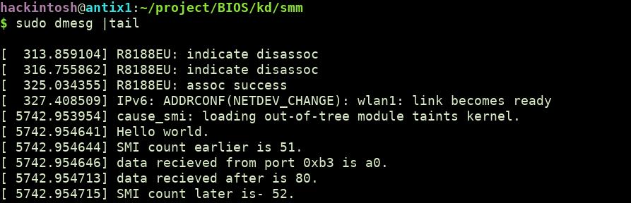
Load the driver using insmod and check the debug messages using dmesg command. Did you see any change after the code is executed?
You will not see any changes in system since the cpu transfer to SMM mode and exited from that quickly without the end user knowing it.
Check SMI count - To confirm that our driver is triggering SMI, we can use SMI_COUNT MSR. Let's modify our code to check if the SMI counter has increased or not.
#define MSR_SMI_COUNT			0x00000034


static int my_init(void)
{


    uint8_t smm_response  = 0x0;
	uint32_t smi_count = 0x0;
    printk(KERN_INFO "Hello world.\n");

    // check smi count
    rdmsrl(MSR_SMI_COUNT, smi_count);
    printk(KERN_INFO "SMI count earlier is %x.\n", smi_count);
    //check the initial value recieve from 0xB3 port
	smm_response = inb(0xb2);

	printk(KERN_INFO "data recieved from port 0xb2 is %x.\n", smm_response);
	//write to 0xB2 port to cause SMI
	outb(0x80, 0xb2);
	// Check the respose in port 0xB3
	smm_response = inb(0xb2);

	printk(KERN_INFO "data recieved after is %x.\n", smm_response);

	rdmsrl(MSR_SMI_COUNT, smi_count);
    printk(KERN_INFO "SMI count later is- %x.\n", smi_count);

    return  0;
}

static void my_exit(void)
{
    printk(KERN_INFO "Goodbye world.\n");

    return;
}

module_init(my_init);
module_exit(my_exit);

MODULE_LICENSE("GPL");
MODULE_AUTHOR("Shubham Dubey <shubham0d@protonmail.coms>");
MODULE_DESCRIPTION("SMM interaction");
Let load the driver and check the debug messages.
You can check that SMI count has increased after writing to port 0xB2. There are many other events that can be trigger from operating system to generate SMI like programming the local APIC or writing to some other ports. You can consult your chipset datasheet to know more about that.
SMRAM
SMM code stays in a special protected memory region called SMRAM. This address space contains the SMI handler code and data, this handler code is the first code to execute when SMI is triggered. SMRAM can be locked so that even the privileged software in the protected mode of the CPU cannot access it.
Structure of SMRAM
First off, few terms used in context of SMRAM:
SMBASE: It is a cpu internal register that contains the base address of SMRAM for a processor.
SMI Handler code: This is the first code that get executed on SMI trigger. It is at specific offset from SMBASE.
State saved area: When switching to SMM the cpu state is saved on SMM at particular offset from SMBASE. Before exiting from SMM, processor state is restored by loading the saved state from SMRAM back to processor registers.
The default SMRAM size is 64 KBytes . The SMBASE default value at system startup/ hardware reset is 0x30000. The processor looks for the first instruction of the SMI handler at the address [SMBASE + 0x8000]. It stores the processor’s state in the area from [SMBASE + 0xFE00] to [SMBASE + 0xFFFF].
Even the startup SMBASE is fixed, it can be relocated by changing SMBASE register which is present at memory offset [SMBASE+ 0xFEF8]. It should be clear that since the SMBASE is inside SMRAM, it can only be modified when in SMM.
A layout of SMRAM looks like below:
Multi-core systems will typically have their SMBASE offset differ by N bytes from each other. For example: Core 0 defines SMBASE as 0xA0000, will enter SMI handler at 0xA8000 – Core 1 defines SMBASE as 0xA1000, will enter SMI handler at 0xA9000 etc.
Some registers in the SMRAM state save area may be read and changed by the SMI handler, with the changed values restored to the processor registers by the RSM instruction. Some register images are read-only, and must not be modified. Below is the mapping of registers in saved state area.
You can see SMBASE register field at offset 0x7EF8 in above list.
Finding SMBASE
In this part we will try to find the possible SMRAM memory location. It can be located anywhere in the 4GB memory (to be precise it will be <TOLUD). SMRAM must relocate at least once after system boot from 0x30000 to any other memory space.
For older systems(ICH chipset based) SMRAM is present at atleast one of the following SMM region:
For newer chipset (PCH one), the SMM region is limited to Compatible and TSEG region.
To keep things recent, we will only discuss the Compatible and TSEG regions.
Compatible SMRAM space
Its fixed address space ( 0xA0000 - 0xBFFFF) in physical memory. When compatible SMM space is enabled, SMM-mode processor accesses to this range are routed to physical system memory at this address. Non-SMM-mode processor accesses to this range are considered to be the video buffer area.
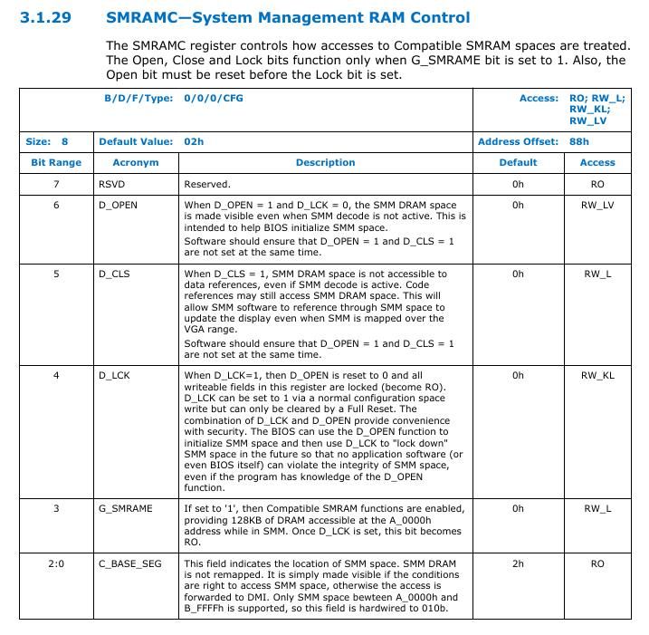
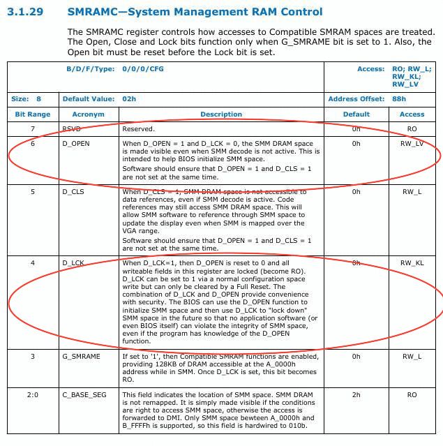
To check if compatible SMRAM is enabled intel processors have G_SMRAME flag present on SMRAMC register. SMRAMC register is present at DRAM controller(0:0:0) at offset 0x88. It may differ for your processor, verify it on datasheet.
Let's create a linux driver to check if compatible SMRAM is enabled.
static int my_init(void)
{
	struct pci_dev *dev;
	u8 pci_data;
    printk(KERN_INFO "Hello world.\n");
    //get pci device
    dev = pci_get_device(0x8086, 0x0a04, NULL);
    if (!dev)
    {
		printk(KERN_INFO "FAILED to get pci device\n");
		pci_dev_put(dev);
		return -ENODEV;
	}
	printk(KERN_INFO "Attached to the pci device\n");
	//Offset 0x88 in DRAM controller
	pci_read_config_byte(dev, 0x88, &pci_data);
	printk(KERN_INFO "SMRAMC data recieved is 0x%x.\n", pci_data);


	// Bit 3 in SMRAMC is G_SMRAME
	pci_data = pci_data >> 3;
	pci_data = pci_data & 0x1;
	printk(KERN_INFO "G_SMRAME is set to %x.\n", pci_data);

	//cleanup after use
	pci_dev_put(dev);


    return  0;
}
The output I received from dmesg after loading the module:
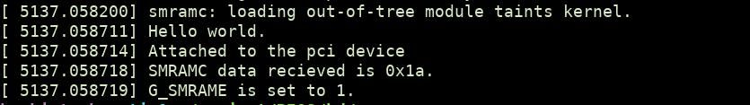
From above, it is confirmed that compatible SMRAM is enabled. We can check the data at memory address 0xA0000 using chipsec.
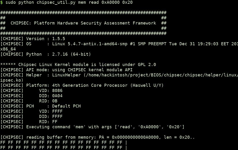
0xFF as bytes confirm the SMRAM presence as SMRAM data is not accessible from the operating system.
Note: You can also read the physical address from kernel module using ioremap call. phys_addr_t comp_smram_phys = 0xA0000;
void __iomem *mapped = ioremap(comp_smram_phys, 0x10); //reading 10 bytesTSEG Space (Top of main memory segment)
TSEG is a variable address space that is present at address TOLUD-STOLEN (discussed below).
Before that let check a graphic representation of main memory:
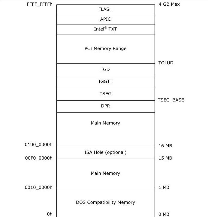
In the above image between TOLUD and TSEG memory space, IGD and IGGTT combined called STOLEN memory. Hence
TSEG = TOLUD - STOLEN - TSEG_SIZE to TOLUD - STOLEN
Let's define the TOLUD and STOLEN first:
TOLUD: Top of Low Usable DRAM
TOLUD register is restricted to 4 GB memory (A[31:20]), but the processor can support up to 32 GB, limited by DRAM pins. It is present at DRAM controller at offset 0xBC.
STOLEN:
STOLEN refer to graphic memory stolen, which is optional and can be 0. STOLEN size can be determined by checking GMS in GGC register which is present at offset 0x50 on DRAM controller.
According to GMS bits, you can determine the size of STOLEN memory and subtract it from TOLUD to get the TSEG end address.
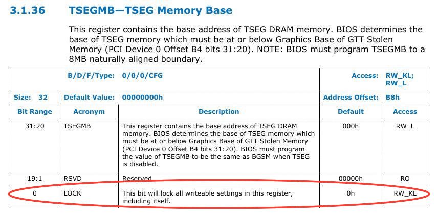
Luckily for PCH processors, you don't have to manually find the TSEG memory by using TOLUD or STOLEN. There is a register TSEGMB that contains the base address of TSEG memory.

In PCH based system STOLEN = DSM size + GSM size.
For STOLEN memory DSM base and GSM base are determined by BDSM and BGSM registers respectively. The registers are present at DRAM controller at offset 0xB0 and 0xB4.
From above data we can conclude that by subtracting TSEG base from BGSM base, we can find the TSEG size. (Note: We are subtracting from BGSM since its lower the BDSM)
Let's write a module to get TSEG base and size.
static int my_init(void)
{
	struct pci_dev *dev;
	u32 pci_data;
	u32 stolen_data;
	u32 tseg_size;
    printk(KERN_INFO "Hello world.\n");
    //get pci device
    dev = pci_get_device(0x8086, 0x0a04, NULL);
    if (!dev)
    {
		printk(KERN_INFO "FAILED to get pci device\n");
		pci_dev_put(dev);
		return -ENODEV;
	}
	printk(KERN_INFO "Attached to the pci device\n");
	//read dword value from pci deevice

	pci_read_config_dword(dev, 0xb8, &pci_data);
	printk(KERN_INFO "TSEGMB register data recieved is 0x%x.\n", pci_data);
	printk(KERN_INFO "TSEGMB is set to 0x%x.\n", (pci_data >> 1) << 1);


	//check base of GTT stolen memory
	pci_read_config_dword(dev, 0xb4, &stolen_data);
	printk(KERN_INFO "BGSM register data recieved is 0x%x.\n", stolen_data);
	printk(KERN_INFO "BGSM is set to 0x%x.\n", (stolen_data >> 1) << 1);

	tseg_size = ((stolen_data >> 1) << 1) - ((pci_data >> 1) << 1);
	printk(KERN_INFO "TSEG size is 0x%x.\n", tseg_size);

	//cleanup after use
	pci_dev_put(dev);


    return  0;
}
The output I received is the following:
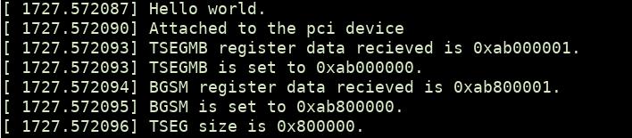
Here, The TSEGMB memory address is 0xab000000 and its size is 0x800000 (8MB).
Note: TSEG size is not equal to SMRAM size.
You can verify if the address is non-readable or not using chipsec like we did it above.
Note: For PCH based system with no HSEG, if TSEG is enable that implies that Compaible range is also enabled.
Protections for SMRAM
The memory controller offers dedicated locks to limit access to SMRAM memory to system firmware (BIOS) only. BIOS after loading the SMM code into SMRAM, can (and should) later "lock down" system configuration in such a way that no further access, from outside the SMM mode, to SMRAM is possible, even for an OS kernel (or a hypervisor).
D_LCK and D_OPEN
Intel provide and D_OPEN and D_LCK bits to make SMRAM region non-accessible from outside SMM.
To help the BIOS configure SMRAM, the chipset provides a means for leaving SMRAM open even when the processor is not in SMM by D_OPEN flag. D_LCK prevents this bit from being asserted. These flags are present on SMRAMC register at bit 4 and 6.
Let's check the flags in our system:
static int my_init(void)
{
struct pci_dev *dev;
u8 pci_data;
printk(KERN_INFO "Hello world.\n");
//get pci device
dev = pci_get_device(0x8086, 0x0a04, NULL);
if (!dev)
{
printk(KERN_INFO "FAILED to get pci device\n");
pci_dev_put(dev);
return -ENODEV;
}
printk(KERN_INFO "Attached to the pci device\n");
//read dword value from pci deevice
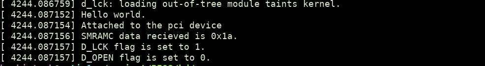
pci_read_config_byte(dev, 0x88, &pci_data);
printk(KERN_INFO "SMRAMC data recieved is 0x%x.\n", pci_data);
// D_LCK bit is 4
// pci_data = pci_data >> 4;
// D_OPEN bit is 6
// pci_data = pci_data >> 6;
printk(KERN_INFO "D_LCK flag is set to %x.\n", (pci_data >> 4) & 1);
printk(KERN_INFO "D_OPEN flag is set to %x.\n", (pci_data >> 6) & 1);
//cleanup after use
pci_dev_put(dev);
return 0;
}I received the following output:
TSEG lock
Even if D_OPEN is set, still outside SMM application will not be able to access the SMRAM present in TSEG region since TSEG is another protected memory area(protected using SMRRs). But the attacker can try to change the TSEG base to shift SMRAM outside TSEG protected region. TSEGMB register contain a lock to prevent that. I.E when its set, the register became read only.
SMRR (System Management Range register)
Another latest(still quite old) and important protection available for SMRAM is SMRR registers which protect SMRAM against multiple types of attacks like SMM cache poisoning, which we will be discussing in next section.
SMRR was introduced for x64 processors. It is used to restrict access to address range defined in SMRR against those range use in MTRR (discussed later) or remapping registers. SMRRs can be modified only when the processor is in SMM.
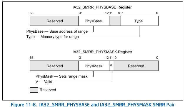
If IA32_MTRRCAP[bit 11] is set, the processor supports the SMRR interface to restrict access to a specified memory address range used by SMM. The system-management range registers consist of a pair of MSRs. The IA32_SMRR_PHYSBASE MSR defines the base address for the SMRAM memory range and the memory type used to access it in SMM. The IA32_SMRR_PHYSMASK MSR contains a valid bit and a mask that determines the SMRAM address range protected by the SMRR interface. These MSRs may be written only in SMM; an attempt to write them outside of SMM causes a general-protection exception.
Lets write a module to check if SMRR is set or not and what physical base it is protecting.
#define MSR_MTRRcap			0x000000fe

#define IA32_SMRR_PHYBASE		0x1F2
#define IA32_SMRR_PHYMASK		0x1F3
static int my_init(void)
{

	uint64_t smrr_base = 0x0;
	uint64_t smrr_mask = 0x0;
	uint64_t mtrr_cap = 0x0;
	uint8_t smrr_support = 0x0;
    printk(KERN_INFO "Hello world.\n");
    rdmsrl(MSR_MTRRcap, mtrr_cap);

	// bit 11 SMRR supported
    smrr_support = (mtrr_cap >> 11) & 0x1;
    printk(KERN_INFO "SMRR support is %x.\n", smrr_support);
    // check SMRRs value
    rdmsrl(IA32_SMRR_PHYBASE, smrr_base);
	rdmsrl(IA32_SMRR_PHYMASK, smrr_mask);
    printk(KERN_INFO "SMRR base is %llx.\n", (smrr_base >> 8) << 8);
    printk(KERN_INFO "SMRR mask is %llx.\n", smrr_mask);


    return  0;
}
After loading, I recieved the following output:

Note that the base address we received is the base address of TSEG region. It is because SMRR protects TSEG region.
Another point to note here is that each CPU has it's SMRR but mostly you will find each SMRR[X] have same base and mast set.
Breaking Security of SMM
So far we have covered the basics of SMM and where they are mapped in our physical memory. Now lets check the known attacks on SMM which are found in past by different researchers. All of these attacks are old and fixed in most recent processors, but we are covering them to give you the understanding about SMM security.
Unlocked SMM
In older systems (without SMRR) SMM is protected using D_LCK only. There are cases (statically very rare) where vendor forget to set the D_LCK and set the D_OPEN to 1. In these cases SMM space is unlocked and writable from outside SMM.
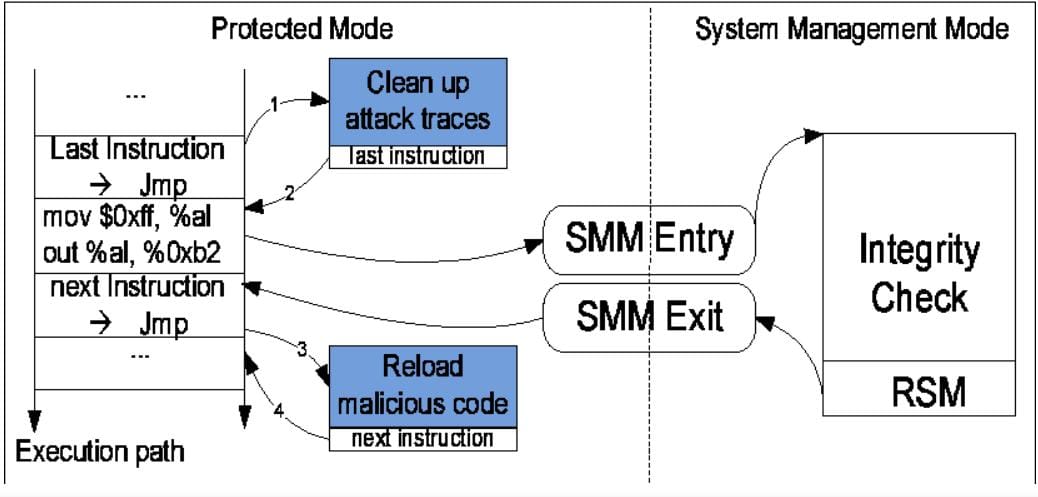
There are few proof of concept rootkits called SMBR that leverage this fact to install a new SMI handler that perform malicious activity like network monitoring, data exfiltration etc. Here is decribed steps mentioned in one of the research paper (link on references) related to SMM rootkits.
- On a host machine, an attacker makes SMRAM visible from protected mode for reading and writing by setting the D_OPEN bit.
- Once D_OPEN is set, the attacker copies the rootkit SMM handler code to the handler portion ofSMRAM as defined by the Intel documentation.
- Finally, the attacker clears the D_OPEN bit and sets the D_LCK bit. This has the effect of making SMRAM invisible to everything other than the subverted (rootkit) SMI handler and of locking the SMRAMC register so that it can no longer be modified. The addressing of the SMRAMC register is chipset specific.
You can watch the whole talk on the topic here:
Jumping from SMI to unprotected region
SMI handler code are mostly written by intel but modified further by vendors. There can be time where SMI handler code call/refer code or data of non SMRAM region. This can have catastrophic effect since that region can be controlled by attacker. Few points on this from opensecuritytraining BIOS course (link below):
ITL found multiple bugs in Intel's SMM code where it was accessing data outside the protected ranges, which could consequently be attacker controlled (which led to simple "change a function pointer to jump to my code" type attacks, and could lead to buffer overflow attacks)
You can learn more on this topic from this talk (although the talk is for non security audions but covers lots of interesting use of SMI handler code and issues to look for while writting those):
More than that, vendors are allowed to put complex capabilities in SMI handler code like setting paging, protected mode etc (even more complex stuff). Having such complex code in SMI is always a bad idea. Wrong register setup or memory access can cause a big hole in SMM protection.
SMM Cache poisioning
This is a well known attack discovered by Invisible things labs in 2009. It leverages the fact that caching is enabled even in SMM. To understand more about this attack we first need to know how Intel caches a region of memory using MTRR.
MTRR and memory caching type
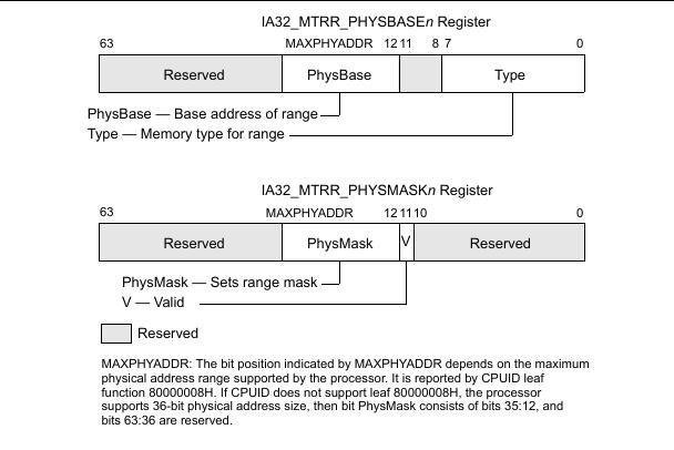
Intel processors provide functionality to set type of caching for a region of memory using few MSR called MTRRs (they are multiple in number). The MSRs are named as IA32_MTRR_PHYSBASEn and IA32_MTRR_PHYSMASKn, having following structure.
Type field in MTRR_PHYSBASE can be one of the following:
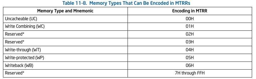
From all these, the one we are interested in is WriteBack which is set by default for a region in most cases.
Writeback Caching: When set for a memory region, read/write are perform from the cache and later write-back into memory. It is used to reduce the bus traffic between processor and memory. In brief: when you read something from the memory with WB set, it gets read from cache line. Similarly, when you write something to that memory, it gets written to the cache line and later written back to memory.
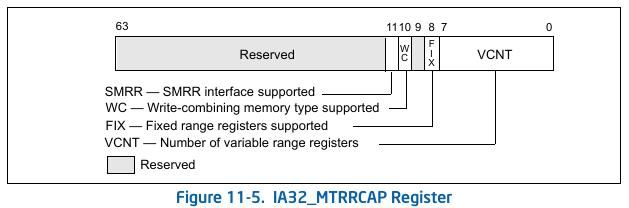
Before moving forward to attack, let's write a module to check MTRR status. Intel contain IA32_MTRRCAP MSR that contain info like amount of MTRR in the processor and if SMRR enable etc.
Lets write our code keeping in mind above structure:
#define MSR_MTRRcap			0x000000fe

#define IA32_MTRR_PHYBASE0		0x200
#define IA32_MTRR_PHYMASK0		0x201
#define IA32_MTRR_PHYBASE1		0x202
#define IA32_MTRR_PHYMASK1		0x203
static int my_init(void)
{

	uint64_t mtrr_base = 0x0;
	uint64_t mtrr_mask = 0x0;
	uint64_t mtrr_cap = 0x0;
	uint8_t  mtrr_supported = 0x0;
	uint8_t  fix_range_mtrr = 0x0;
	uint8_t  wc_support = 0x0;
	uint8_t smrr_support = 0x0;
    printk(KERN_INFO "Hello world.\n");
    rdmsrl(MSR_MTRRcap, mtrr_cap);
    // check the defined fields inside IA32_MTRRCAP
    // bit 7:0 MTRR_PHYBASEX can be used
	// bit 8 Fixed Range MTRR are supported
	// bit 10 WC supported
	// bit 11 SMRR supported
	// bit 11 PRMMR supported
    mtrr_supported = mtrr_cap & 0xFF;
    fix_range_mtrr = (mtrr_cap >> 8) & 0x1;
    wc_support = (mtrr_cap >> 10) & 0x1;
    smrr_support = (mtrr_cap >> 11) & 0x1;
    printk(KERN_INFO "MTRRCAP is %llx.\n", mtrr_cap);
    printk(KERN_INFO "Number of MTRR is %d.\n", mtrr_supported);
    printk(KERN_INFO "Fixed range MTRR support is %x.\n", fix_range_mtrr);
    printk(KERN_INFO "WC support is %x.\n", wc_support);
    printk(KERN_INFO "SMRR support is %x.\n", smrr_support);
    // check MTRRs value
    rdmsrl(IA32_MTRR_PHYBASE0, mtrr_base);
	rdmsrl(IA32_MTRR_PHYMASK0, mtrr_mask);
    printk(KERN_INFO "MTRR Physical base 0 is %llx.\n", mtrr_base);
    printk(KERN_INFO "MTRR Physical Mask 0 is %llx.\n", mtrr_mask);


    return  0;
}
The output I recieved is following:
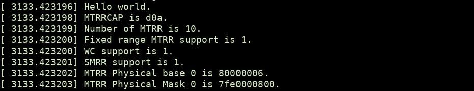
6 at end of base represent WB set. Base is 0 for data 80000000.
Now lets move to our cache poising attack study. Basic idea is when the cpu is not in SMM, the cpu cannot write to SMRAM. But if the SMRAM is cached in Write back mode by modifying MTRR to cache SMRAM memory, the cpu only write to the cached version and not in memory. Now, when later SMI occur, the cpu will execute the SMI handler code from cache rather than from SMRAM. Below is the steps mentioned in the research paper by ITL:
- The attacker should first modify system MTRR register(s) in order to mark the region of system memory where the SMRAM is located as cacheable with type Write-Back (WB).
- Attacker now generates write accesses to physical addresses corresponding to locations where the SMRAM is located. Those accesses will now be cached, because we have marked this range of physical addresses as WB cacheable. Normally, physical addresses corresponding to the location of SMRAM would be un-cacheable and any write accesses to these addresses would be dropped by the memory controller (chipset).
- Finally attacker needs to trigger an SMI, which will transfer execution to the SMM code. The CPU will start executing the SMM code, but will be fetching the instructions from the cache first, before reading them from DRAM. Because the attacker previously (in point #2) generated write access to SMRAM locations, the CPU will fetch attacker-provided data from the cache and execute them as an SMI handler, with full SMM privileges.
To prevent this attack Intel has introduced SMRR registers (already discussed above) in 64 bit architecture. SMRR restricts access to the address range defined in the SMRR registers and it takes priority over MTRR in case of overlapping ranges.
APIC Remapping attack
This is the most recent attack introduced in 2015 by Christopher Domas. To learn about this, we need to first understand the basics of APIC.
Advanced Programmable Interrupt Controller (APIC) is used to transfer interrupts from PCI devices to processor or in between processors. There are two types of APIC - I/O APIC and local APIC.
I/O APIC - The external I/O APIC is part of Intel’s system chip set. Its primary function is to receive external interrupt events from the system and its associated I/O devices and relay them to the local APIC as interrupt messages.
Local APIC - It receives interrupts from the processor’s interrupt pins, from internal sources and from an external I/O APIC (or other external interrupt controller). It sends these to the processor core for handling. In multiple processor (MP) systems, it sends and receives interprocessor interrupt (IPI) messages to and from other logical processors on the system bus. IPI messages can be used to distribute interrupts among the processors in the system or to execute system wide functions (such as, booting up processors or distributing work among a group of processors).
For this attack, we only care about the local APIC. Software interacts with the local APIC by reading and writing its registers present in Local APIC memory space. APIC registers are memory-mapped to a 4-KByte region of the processor’s physical address space with an initial starting address of 0xFEE00000. The structure of local APIC memory looks like this
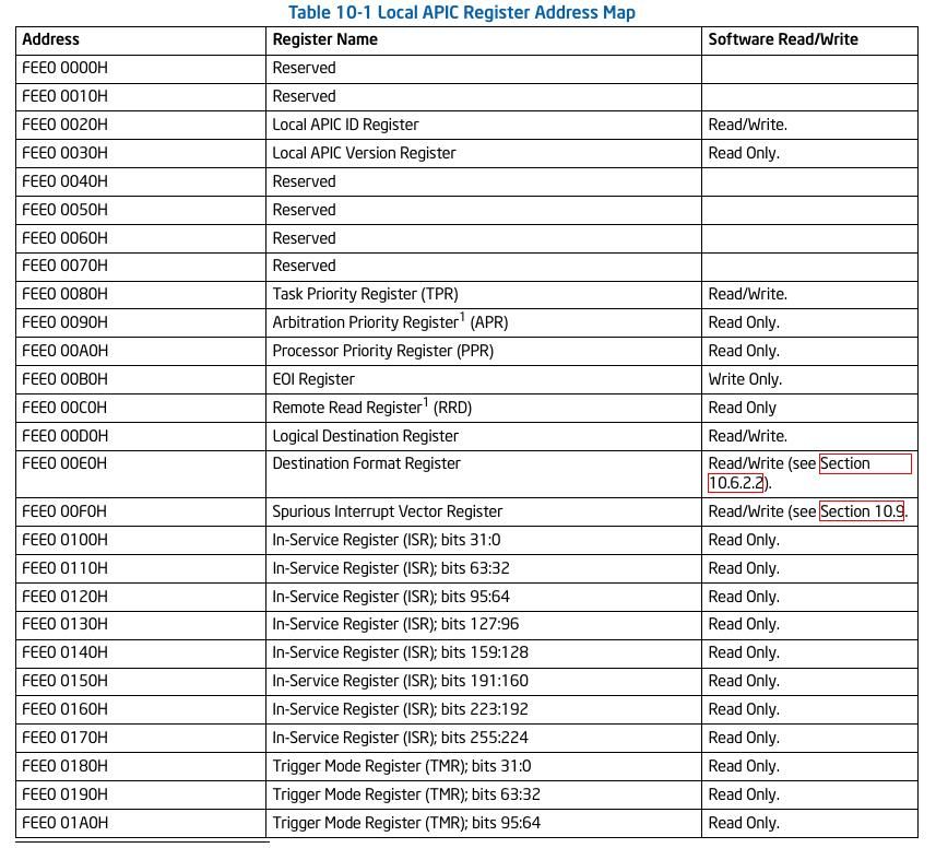
The list of memory map goes beyond the above image. You will found that a lot of registers here are writable. Moving forward, the most important point about local APIC is, it's relocatable. Using IA32_APIC_BASE MSR someone can enable/disable local APIC as well as rebase it.
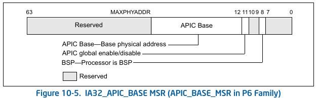
Domas has found that in x86 processors if APIC base is set to SMRAM base, the memory address will belong to local APIC memory. Hence on next SMI, the code from APIC will get executed since the read request will go to local APIC first which is in procesor rather than to controller where SMRAM is present. Since, lots of local APIC memory bytes are writable, attacker can write a well crafted payload in APIC memory to execute its code.
You can learn more about this attack from this talk:
You can write a simple module to modify APIC base:
#define IA32_APIC_BASE		0x1B


static int my_init(void)
{
	uint64_t apic_base = 0x0;
	uint8_t apic_global = 0;
	uint32_t apic_base_addr = 0;
	uint64_t new_apic_base = 0;
	printk(KERN_INFO "Hello world!.\n");


    rdmsrl(IA32_APIC_BASE, apic_base);
    printk(KERN_INFO "APIC_BASE return %llx.\n", apic_base);
    apic_global = (apic_base >> 11) & 1;
    // change the constant value
    new_apic_base = 0xab000000 | (apic_global << 11);
    wrmsrl(IA32_APIC_BASE, new_apic_base);
    apic_base = 0;

    rdmsrl(IA32_APIC_BASE, apic_base);
    printk(KERN_INFO "APIC_BASE updated to %llx.\n", apic_base);
    return  0;
}
Intel has patched the vulnerability by checking local APIC base with SMRR base while relocating the local APIC. In case the requested base is in the memory address protected by SMRR than the rebase will fail. Hence, most probably if your processor is patched, trying to execute above module will cause a system crash.
Having Vulnerable BIOS
The final attack ( and most obvious one) against SMM is the weakness of BIOS. Since SMM code resides in BIOS image, even if the SMRAM is secure, having vulnerable BIOS makes it useless since someone can modify the BIOS, hence SMRAM code.
There are few other great vulnerability found in last few years in SMM that we haven't cover. I recommend checking them yourself. We are ending this article here only. You can find the sample codes used in this article here. Stay tuned for more posts on this series.
References and Further resources:
Opensecuritytraining BIOS course: https://opensecuritytraining.info/IntroBIOS.html
Intel software developer manual: https://software.intel.com/content/www/us/en/develop/articles/intel-sdm.html
SMM rootkit: a new breed of OS independent malware: https://onlinelibrary.wiley.com/doi/pdf/10.1002/sec.166
SMM cache fun: https://invisiblethingslab.com/resources/misc09/smm_cache_fun.pdf